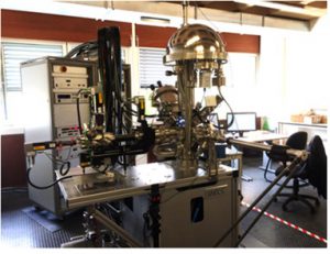
X-ray Photoelectron Spectroscopy (XPS)
TEMA – UA / 1st Workshop on Characterization and Analysis of Nanomaterials University of Aveiro, Portugal July 9, 2019
Coordinator: Dr. Gonzalo Guillermo Otero Irurueta
otero.gonzalo@ua.pt
TEMA (DEM – University of Aveiro) has a multi-technique system working under Ultra High Vacuum conditions. Among others, the main experimental characterization techniques are:
- High resolution XPS – resolution of 0.5 eV
- High resolution UPS – resolution of 0.14 eV
- Auger electron spectroscopy (AES)

Flexible modular analysis system
X-ray Photoelectron Spectroscopy (XPS) is a surface-sensitive spectroscopic technique (about 1-10 nm depth) that detects the kinetic energy of the photoelectrons emitted by a surface when irradiated by X-ray. This way, it allows to obtain information about the elemental composition and chemical environment of the elements present within the surface of a material.
XPS can be used to analyze a great variety of compounds, such as thin films, 2D materials, metal alloys, semiconductors, coatings, catalysts, inorganic oxides, pollutants, polymers, bio-materials, organic-inorganic hybrids…
The main features of our system are:
- Ultra clean environment (P < 2×10⁻¹⁰ mbar)
- Monocromatic Al Kα X-ray source (1486.71 eV)
- UV lamp for UPS measurements (with He I and He II)
- High resolution electron energy analyzer. Standard spot size of 2 mm and 0.2 mm
- 1-D delayline detector
- Electron gun for AES with variable energy (Emax= 4.5 kV). The electron gun is also used at low energy for charge compensation in the case of soft insulating samples.
- 5 axis (X, Y, Z, polar and azimuthal) high precision manipulator (motorized and PC controlled)
- Independent Fast Entry chamber. 30 min is the typical time needed for introducing a sample in the main chamber
- Sputtering gun working with Ar+ ions of variable energy (0.5 – 3 kV) and variable dose. As an example, at 1.5 kV it is possible to remove 100 nm of a sample per hour.


