


Scaning electron microscope (SEM) / 1st Workshop on Characterization and Analysis of Nanomaterials University of Aveiro, Portugal July 9, 2019
Coordinator: Nuno André Fraga de Almeida
nunodealmeida@ua.pt

SEM images obtained using a Hitachi, TM4000Plus microscope
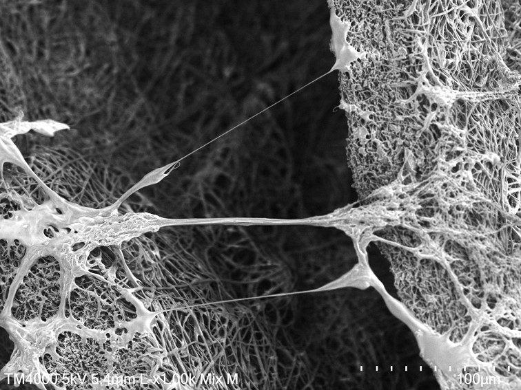 A chondrocyte cell bridging two fibrous layers of a 3D electrospun scaffold after 7 days in cA chondrocyte cell bridging two fibrous layers of a 3D electrospun scaffold after 7 days in culture. The topographical cues modulate the cell morphology, leading to the formation of extended filopodia capable of supporting an enhanced 3D cell migration.ulture. The topographical cues modulate the cell morphology, leading to the formation of extended filopodia capable of supporting an enhanced 3D cell migration.
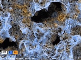 EDS mapping obtained from a composite cathode based on Ca3Co4O9 and PrOx for Solid oxide fuel cells (SOFCs).
SEM Principle
Scanning electron microscope (SEM) is an electron microscope that uses a focused beam of electrons to create images of a sample. The image is created using a raster scan pattern, the detected signal and the position of the bean are combined to produce an image.
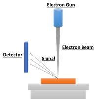
The interaction of the electrons with the sample, produces several signals that contains information about surface topography, atomic weight and surface chemistry.
SEM equipment characteristics
- Accommodates sample sizes of up to 80 mm in diameter and 50 mm in thickness.
- Magnification:
- ×10~×100,000 (Photographic magnification)
- ×25~×250,000 (Monitor display magnification)
- Accelerating voltage 5 kV, 10 kV, 15 kV
- Image signals.
- Backscattered electrons (BSE)
- Secondary electrons (SE)
- Mix (Backscattered electrons + Secondary electrons)
- X-rays (Energy-dispersive X-ray spectroscopy-EDX)
- Vacuum mode:
- BSE: Conductor/Standard/Charge-up reduction
- SE: Standard/Charge-up reduction
- Mix: Standard/Charge-up reduction